Sunday, April 18, 2021

SoC Integration Testing: Hw/Sw Coordination (Part 2)


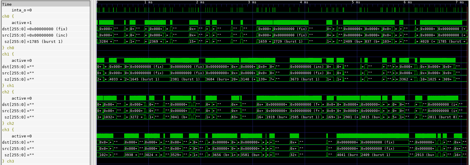
Controlling the outside world -- specifically interface BFMs -- from embedded software is critical to SoC integration tests that exercise interface IP. In the last post, we showed how to pass data from embedded software to Python by tracing execution of the processor core and reading the mirrored values of registers and memory to obtain parameter values. While functional, doing things in this way is highly specific to one message-passing approach and is pretty labor intensive. In this post, we'll add some abstraction and automation to improve usability and scalability.


Design Goals


While we're initially focused on providing a nice automated way to communicate between embedded software and the test harness in a simulation environment, the design goals go beyond this. The diagram above shows the basic architecture. Endpoints provide a portal for one environment to call APIs in another environment. Each endpoint supports a known set of APIs, and different endpoints will support different sets of APIs. 

Each environment interacts with APIs on an endpoint without needing to know how communication is implemented. For example, execution trace might be used to implement processor to Python communication in a simulation-based environment. When the design is synthesized to FPGA, communication might be implemented via an external interface. With appropriate abstraction, neither the test software running on the processor nor the Python test code should need to change despite the fact that data is being moved in very different ways. 

In order for this to be feasible, we'll need to collect some meta-data about the APIs.


Example

I always find an example to be helpful, so let's look at the enhancements to the flow in the context of a simple example.


The diagram above shows the key elements of a very small SoC called Tiny SoC. We can test many aspects of integration using just software on the processor. For example, we can read registers in the peripheral devices and check that they are correct. We can carry out DMA transfers. But, we need to control the outside world when testing the full path from software through the UART and SPI devices.

Bus functional models (BFMs) or Verification IP (VIP) provide very effective ways to interact with interface protocols from testbench code. What we need in addition is a way to control these BFMs from the software running on the core in the design.


Capturing the API

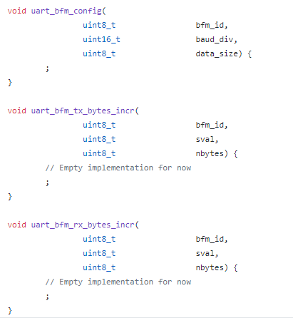
Let's focus on the UART for now. Our UART BFM provides a detailed API for configuring individual attributes of the UART protocol (eg baud-rate divisor) and for interacting with the UART protocol a byte at a time. That's fine for IP-level testing, but is a bit too low-level for software-driven testing.

For software-driven testing, we want to instruct the BFM to do some reasonable amount of work and let it go. To help with this, the UART BFM defines a higher-level API intended for use by software. 

An example of that higher-level API is shown above. Calling the uart_bfm_tx_bytes_incr API causes the BFM to begin sending a stream of bytes starting with a specific value and incrementing. There is another API that instructs the BFM to expect to receive a stream of bytes sent by the software running on the processor.

To enable automation, we describe the Python API that we will call from embedded software using special annotations. We collect related APIs together in a class, and identify whether these methods are exported by the Python environment and will be called by the embedded software, or are imported by the Python and will be called by Python code. 


Since we want embedded software to call this API, the API is considered to be exported by Python. You can also see the configuration function that updates the UART's configuration (eg baud rate).

Each of the method parameters is given a Python3 type annotation. This enables the Python libraries to know the type of each parameter and collect the right data to pass when the functions are called. 

On the C side, we simply need to have functions with the same signature as what we've captured in the Python API definition.


While the code shown above (link) is hand-coded, we could generate it automatically based on what is specified in the Python API definition. 


Connecting to Implementation: Python

Connecting all of this up on the Python side involves connecting the relevant BFMs and API implementations together. 


The snippet above is from the cocotb test that runs when a baremetal software test is run (link). At the beginning of simulation, the test locates the relevant BFMs. The u_dbg_bfm is the tracer BFM that monitors execution of software on the processor core. This BFM implements an Endpoint, as shown in the diagram at the beginning of the post. The u_uart_bfm is the BFM connected to the UART interface on TinySoC. 

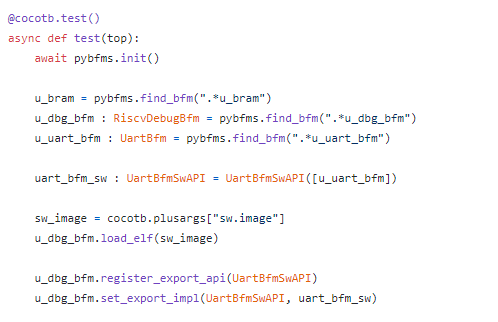
Once we have all the BFMs, we can create an instance of the higher-level UART BFM API (uart_bfm_sw) and tell the debug BFM that it should handle the embedded software calling these APIs.


Example C-Test
With the BFMs connected on the Python side, we can now focus on how to interact with the BFM from the software test.

The software test snippet above transmits some data via the UART to the waiting UART BFM to check (link). Before we can send data, both the UART IP and the external BFM need to be configured in the same way. We program the UART IP via its registers, and call the uart_bfm_config function to cause the corresponding Python method to be invoked. This will cause the UART BFM mode to be configured.

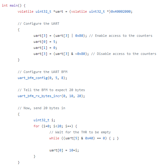
Next, we call the uart_bfm_rx_bytes_incr to tell the UART BFM that it should expect to receive 20 bytes. It should expect the first byte to have a value 10 and subsequent bytes to increment by one. By telling the BFM what to expect, our test is self-checking and the required amount of interaction is small.

Finally, we again interact with the UART IP actually send the data that the BFM is expecting. 

Next Steps
The API definition and Endpoint architecture described in the post above provides a modular way to capture the APIs used to communicate across environments. Because the API signature is captured in machine-readable way, it also enables the use of automation when implementing the APIs for different environments. 

As I mentioned at the beginning of the post, the API and Endpoint architecture is designed so it can be applied in many verification environments -- it's certainly not restricted to just communicating between embedded software test and the test harness. I've been interested for a while in methodology for creating and verifying firmware along with the IP that it controls such that it's ready to go when SoC-integration testing begins. My next post will begin exploring how to create, verify, and deliver firmware along with an IP.

References


Disclaimer
The views and opinions expressed above are solely those of the author and do not represent those of my employer or any other party.

Sunday, March 28, 2021

SoC Integration Testing: Hw/Sw Test Coordination (Part 1)


IP- and subsystem-level testbenches are quite monolithic. There is a single entity (the testbench) that applies stimulus to the design, collects metrics, and checks results. In contrast, an SoC-level testbench is composed of at least two islands: the software running on the design’s processor and the external testbench connected to the design interfaces. Efficiently developing SoC tests involving both islands requires the ability to easily and efficiently coordinate their activity.

There are a two times when it’s imperative that the behavior of the test island(s) inside the design and the test island outside the design are coordinated – specifically, the beginning and end of the test when all islands must be in agreement. But, there are many other points in time where it is advantageous to be able communicate between the test islands. 

Especially when running in simulation, the ability to efficiently pass debug information from software out to the test harness dramatically speeds debug. 

It’s often useful to collect metrics on what’s happening in the software environment during test – think of this as functional coverage for software. 

Verifying our design requires applying external stimulus to prove that the design (including firmware) reacts appropriately. This requires the ability to coordinate between initiating traffic on external interfaces and running firmware on the design processors to react – another excellent application of hardware/software coordination. 

Often, checking results consumes a particularly-large portion of the software-test’s time. The ability to offload this to the test harness (which runs on the host server) can shorten our simulation times significantly. 

Key Care-Abouts

When it comes to our key requirements for communication, one of the biggest is efficiency – at least while we’re in simulation. The key metric being how many clock cycles it takes to transfer data from software to testbench. When we look at a simulation log, we want to see most activity (and simulation time) focused on actually testing our SoC, and not on sending debug messages back to the test harness. A mechanism with a low overhead will allow us to collect more debug data, check more results, and generally have more flexibility and freedom in transferring data between the two islands.

Non-Invasive

One approach to efficiency is to use custom hardware for communication. Currently, though this may change, building the communication path into the design seems to be disfavored. So, having the communication path be non-invasive is a big plus.

Portable

Designs, of course, don’t stay in simulation forever. The end goal is to run them in emulation and prototyping for performance validation, then eventually on real silicon where validation continues -- just at much higher execution speed. Ideally, our communication path will be portable across these changes in environment. The low-level transport may change – for example, we may move from a shared-memory mailbox to using an external interface – but we shouldn’t need to fundamentally change our embedded software tests or the test behavior running on the test harness.

Scalable

A key consideration – which really has nothing to do with the communication medium at all – is how scalable the solution is in general. How much work is required to add a piece of data (message, function, etc) that will be communicated? How much specialized expertise is required? The simpler the process is to incrementally enhance the data communicated, the greater the likelihood that it will be used.

Current Approaches

Of the approaches that I’ve seen in use, most involve either software-accessible memory or the use of an existing external interface as the transport mechanism between software and the external test harness. In fact, one of the earliest cases of hardware/software interaction that I used was the Arm Trickbox – a memory-mapped special-purpose hardware device that supported sending messages to the simulation transcript and terminating the test, among other actions.

In both of these cases, some amount of code will run on the processor to format messages and put them in the mailbox or send them via the interface. 

Challenges

Using a memory-based communication is generally possible in a simulation-based environment – provided we can snoop writes to memory, and/or read memory contents directly from the test harness. That doesn’t mean that memory-based communication is efficient, though, and in simulation, we care a lot about efficiency due to the speed of hardware simulators.

Our first challenge comes from the fact that all data coming from the software environment needs to be copied from its original location in memory into the shared-memory mailbox. This is because the test harness only has access to portions of the address space, and generally can’t piece together data stored in caches. The result is that we have to copy all data sent from software to the test harness out to main (non-cached) memory. Accessing main memory is slow, and thus communication between software and the test harness significantly lengthens our simulations.

Our second challenge comes from the fact that the mailbox is likely to be smaller than the largest message we wish to send. This means that our libraries on both sides of the mailbox need to manage synchronizing data transmission with available space in the mailbox. This means that one of the first tasks we need to undertake when bringing up our SoC is to test the communication path between software and test harness.

A final challenge, which really ought not to be a challenge, is that we’ll often end up custom-developing the communication mechanism since there aren’t readily-available reusable libraries that we can easily deploy. More about that later.

Making use of Execution Trace

In a previous post, I wrote about using processor-execution trace for enhanced debug. I've also used processor trace as a simple way to detect test termination. For example, here is the Python test-harness code that terminates the test when one of 'test_pass' or 'test_fail' are invoked:

In order to support test-result checking, the processor-execution trace BFM has the ability to track both the register state and memory state as execution proceeds.


The memory mirror is a sparse memory model that contains only the data that the core is actively using. It's initialized from the software image loaded into simulation memory, and updated when the core performs a write. The memory mirror provides the view of memory from the processor core's perspective -- in other words, pre-cache. 

Our test harness has access to the processor core's view of register values and memory content at the point that a function is called. As it turns out, we can build on this to create a very efficient way to transferring data from software to the test harness.

In order to access the value of function parameters, we need to know the calling convention for our processor core. Here's the table describing register usage in the RISC-V calling convention:

Note that x10-17 are used to pass the first eight function arguments. 

Creating Abstraction
We could, of course, directly access registers and memory from our test-harness code to get the value of function parameters. But, a little abstraction will help us out in the long run.

The architecture-independent core-debug BFM defines a class API for accessing the value of function parameters. This is very similar to the varadic-argument API used in C programming:


Now, we just need to implement a RISC-V specific version of this API in order to simplify accessing function parameter values:

Here's how we use this implementation. Assume we have a embedded-software function like this:
When we detect that this function has been called, we can access the value of the string passed to the function from the test harness like this:


Advantages
There are several advantages to using a trace-driven approach to data communication between processor core and test harness. Because the trace BFM sees the processor's view of memory, there's no need to (slowly) copy data out to main memory in order for the test harness to see it. This allows data to stay in caches and avoids unnecessary copying.

Perhaps more importantly, our trace-based communication mechanism allow us to offload data processing to the test harness. Take, for example, the very-common debug printf:


The user passes a format string and then a variable number of arguments that will all be converted to string representations that can be displayed. If our communication mechanism is an in-memory mailbox or external interface, we need to perform the string formatting on the design's processor core. If, however, we use the trace-based mechanism for communication, the string formatting can all be done by the test harness in zero simulation time. This allows us to keep our simulations shorter and more-focused on the test at hand, while maximizing the debug and metrics data we collect.


Next Steps

SoC integration tests are distributed tests carried out by islands of test behavior running on the processor(s) and on the test harness controlling the external interfaces. Testing more-interesting scenarios requires coordinating these islands of test functionality. 

In this post, we’ve looked at using execution-trace to implement a high-efficiency mechanism for communicating from embedded test software back to the test harness. While this mechanism is mostly-specific to simulation, it has the advantage of simplifying communication, debug, and metrics collection at this early phase of integration testing when, arguably, we most-need a high degree of visibility. 

While we have an efficient mechanism, we don’t yet has a mechanism that makes it easy to add new APIs (scalable) nor a mechanism that is easily portable to environments that need to use a different transport mechanism.

In the next post, we’ll have a look at putting some structure and abstraction around communication that will help with both of these points.

References

Disclaimer
The views and opinions expressed above are solely those of the author and do not represent those of my employer or any other party.


Sunday, February 28, 2021

SoC Integration Testing: IP-Integrated Debug and Analysis


One of the things I've always liked about side projects is the freedom to stop and explore a topic of interest as it comes up. One such topic that came up for me recently is IP-integrated debug and analysis instrumentation. I started thinking about this after the last post (link) which focused on exposing a higher-abstraction-level view of processor-core execution. My initial approach to doing this involved a separate bus-functional model (BFM) intended to connect to any RISC-V processor core via an interface. After my initial work on this bus-functional model that could be bolted onto a RISC-V core, two things occurred to me:
  • Wouldn't it be helpful if processor cores came with this type of visibility built-in instead of as a separate bolt-on tool?
  • Wouldn't SoC bring-up be simpler if more of the IPs within the SoC exposed an abstracted view of what they were doing internally instead of forcing us to squint at (nearly) meaningless signals and guess?
And, with that, I decided to take a detour to explore this a bit more. Now, it's not unheard of to create an abstracted view of an IP's operation during block-level verification. Often, external monitors that are used to reconstruct aspects of the design state, and that information is used to guide stimulus generation, or as part of correctness checking. Some amount of probing down into the design may also be done.

While this is great for block-level verification, none of this infrastructure can reasonably move forward to the SoC level. That leaves us with extremely limited visibility when trying to debug a failure at SoC level.

If debug and analysis instrumentation were embedded into the IP during its development, an abstracted view of the IP's operation would consistently be available independent of whether it's being verified at block level or whether it's part of a much larger system.

Approach

After experimenting with this a bit, I've concluded that the process of embedding debug and analysis instrumentation within an IP is actually pretty straightforward. The key goals guiding the approach are:
  • Adding instrumentation must impose no overhead when the design is synthesized. 
  • Exposing debug and analysis information must be optional. We don't want to slow down simulation unnecessarily if we're not even taking advantage of the debug information
When adding embedded debug and analysis instrumentation to an IP, our first step is to create a 'socket' within the IP to which we can route the lower-level signals from which we'll construct the higher-level view of the IP's operation. From a design RTL perspective, this socket is an empty module whose ports are all inputs. We instance this 'debug-socket' module in the design and connect the signals of interest to it.

Because the module contains no implementation and only accepts inputs, synthesis tools very efficiently optimize it out. This means that having the debug socket imposes no overhead on the synthesized result.

Of course, we need to plug something into the debug socket. In the example we're about to see, what we put in the socket is a Python-based bus functional model. The same thing could, of course, be done with a SystemVerilog/UVM agent as well.

Example - DMA Engine

Let's look at a simple example of adding instrumentation to an existing IP. Over the years, I've frequently used the wb_dma core from opencores.org as a learning vehicle, and when creating examples. I created my first OVM testbench around the wb_dma core, learned how to migrate to UVM with it, and have even used it in SoC-level examples. 

DMA Block Diagram

The wb_dma IP supports up to 31 DMA channels internally that all communicate with the outside world via two initiator interfaces and are controlled by a register interface. It isn't overly complex, but determining what the DMA engine is attempting to do by observing traffic on the interfaces is a real challenge!

When debugging a potential issue with the DMA, the key pieces of information to have are:
  • When is a channel active? In other words, when does it have pending transfers to perform?
  • When a channel is active, what is it's configuration? In other words, source/destination address, transfer size, etc.
  • When is a channel actually performing transfers?
While there may be additional things we'd like to know, this is a good start.


The waveform trace above shows the abstracted view of operation produced for the DMA engine. Note the groups of traces that each describe what one channel is doing. The dst, src, and sz traces describe how an active channel is configured. If the channel is inactive, these traces are blanked out. The active signal is high when the channel is actually performing transfers. Looking at the duty cycle of the active signals across simultaneously-active channels gives us a good sense for whether a given channel is being given sufficient access to the initiator interfaces. 

Let's dig into the details a bit more on how this is implemented.

DMA Debug/Analysis Socket
We first need to establish a debug/analysis "socket" -- an empty module -- that has access to all the signals we need. In the fwperiph-dma IP (a derivative of the original wb_dma project), this socket is implemented by the fwperiph_dma_debug module


And, that's all we need. The debug/analysis socket has access to:
  • Register writes (adr, dat_w, we)
  • Information on which channel is active (ch_sel, dma_busy)
  • Information on when a transfer completes (dma_done_all)
Note that, within the module, we have an `ifdef block allowing us to instance a module. This is the mechanism via which we insert the actual debug BFM into the design. Ideally, we would use the SystemVerilog bind construct, but this IP is designed to support a pure-Verilog flow. The `ifdef block accomplishes roughly the same thing as a type bind.

Debug/Analysis BFM

The debug/analysis BFM has two components. One is a Verilog module that translates from the low-level signals up to operations such as "write channel 2 CSR" and "transfer on channel 3 complete". This module is about 250 lines of code, much of it of low complexity. 

The other component of the BFM is the Python class that tracks the higher-level view of what channels are active, how they are configured, and ensures that the debug information exposed in signal traces is updated. The Python BFM can also provide callbacks to enable higher-level analysis in Python. The Python BFM is around 150 lines of code. 

So, in total we have ~400 lines of code dedicated to debug and analysis -- a similar amount and style to what might be present in a block-level verification environment. The difference, here, is that this same code is reusable when we move to SoC level. 

Results

Thus far, I've mostly used the waveform-centric view provided by the DMA-controller integrated debug. Visual inspection isn't the most-efficient way to do analysis, but I've already had a couple of 'ah-ha' moments while developing some cocotb-based tests for the DMA controller. 


I was developing a full-traffic test that was intended to keep all DMA channels busy for most of the time when I saw the pattern in the image above. Notice that a transfer starts on each channel (left-hand side), and no other transfers start until all the previously-started transfers are complete (center-screen). Something similar happens on the right-hand side of the trace. Seeing this pattern graphically alerted me that my test was unintentionally waiting for all transfers to complete before starting the next batch, and thus artificially throttling activity on the DMA engine.


With the test issue corrected, the image above shows expected behavior where new transfers start while other channels are still busy.


Looking Forward

I've found the notion of IP-integrated debug and analysis instrumentation very intriguing, and early experience indicates that it's useful in practice. It's certainly true that not all IPs benefit from exposing this type of information, but my feeling is that many that contain complex, potentially-parallel, operations exposed via simple interfaces will. Examples, such as DMA engines, processor cores, and PCIe/USB/Ethernet controllers come to mind. And, think how nice it would be to have IP with this capability built-in!

In this blog post, we've looked at the information exposed via the waveform trace. This is great to debug the IP's behavior -- while it's being verified on its own or during SoC bring-up. At the SoC level, the higher-level information exposed by at the Python level may be even more important. As we move to SoC level, we become increasingly interested in validation -- specifically, confirming that we have configured the various IPs in the design to support the intended use, but not over-configured them and, thus, incurred excess implementation costs. My feeling is that the information exposed at the Python level can help to derive performance metrics to help answer these questions.

This has been a fun detour, and I plan to continue exploring it in the future -- especially, how it can enable higher-level analysis in Python. But, now it's time to look at how we can bring the embedded-software and hardware (Python)  portions of our SoC testbench closer together. Look for that in the new few weeks.

References

Disclaimer
The views and opinions expressed above are solely those of the author and do not represent those of my employer or any other party.


Saturday, January 30, 2021

SoC Integration Testing: Higher-Level Software Debug Visibility


Debug is a key task in any development task. Whether debugging application-level software or a hardware design, a key to productive debug is getting a higher-level view of what is happening in the design. Blindly stepping around in source code or staring at low-level waveforms is rarely a productive approach to debugging. Debug-log messages provide a high-level view of what's happening in an software application, allowing us to better target what source we actually inspect. Testbench logging, coupled with a transaction-level view of interface activity, provides us that higher-level view when verifying IP-level designs. Much of this is lacking when it comes to verifying SoC integration.

Challenges at SoC Level
We face a few unique challenges when doing SoC-integration testing. Software (okay, really firmware) is an integral part of our test environment, but that software is running really really slowly since it is running at RTL-simulation speeds. That makes using debug messages impractical, since simulating execution of the code to produce messages makes our test software run excruciatingly slowly. In addition, the types of issues we are likely to find -- especially early on -- are not at the application-level anyway. 

Processor simulation models often provide some form of execution trace, such as ARM's Tarmac file, which provides us a window into what's happening in the software. The downsides, here, are that we end up having to manually correlate low-level execution with higher-level application execution and what's happening in the waveform. There are also some very nice commercial integrated hardware/software debug tools that dramatically simplify the task of debugging software at the source level and correlating that with what's happening in the hardware design -- well worth checking out if you have access.

RISC-V VIP
At IP level, it's common to use Verification IP to relate the signal-level view of implementation with the more-abstract level we use when developing tests and debugging. It's highly desirable, of course, to be able to use Verification IP across multiple IPs and projects. This requires the existence of a common protocol that VIP can be developed to comprehend. 

If we want VIP that exposes a higher-level view of a processor's execution, we'll need just such a common protocol to interpret. The good news is that there is such a protocol for the RISC-V architecture: the RISC-V Formal Interface (RVFI). As its name suggests, the RISC-V Formal Interface was developed to enable a variety of RISC-V cores to be formally verified using the same library of formal properties. Using the RVFI as our common 'protocol' to understand the execution of a RISC-V processor enables us to develop a Verification IP that supports any processor that implements the RVFI.

RISC-V Debug BFM
The RISC-V Debug BFM is part of the PyBfms project and, like the other Bus-Functional Models within the project, implements low-level behavior in Verilog and higher-level behavior in Python. Like other PyBfms models, the RISC-V Debug BFM works nicely with cocotb testbench environments.

Instruction-Level Trace
Like other BFMs, the Verilog side of the RISC-V Debug BFM contains various mechanics for converting the input signals to a higher-level instruction trace. Consequently, the signals that expose the higher-level view of software execution are collected in a sub-module of the BFM instance.


The image above shows the elements within the debug BFM. The ctxt scope contains the higher-abstraction view of software execution, while the regs scope inside it contains the register state.


The first level of debug visibility that we receive is at the instruction level. The RISC-V Debug BFM exposes a simple disassembly of the executed instructions on the disasm signal within the ctxt scope. Note that you need to set the trace format to ASCII or String (depending on your waveform viewer) to see the disassembly. 


C-Level Execution Trace
Seeing instruction execution and register values is useful, but still leaves us looking at software execution at a very low level. This is very limiting, and especially so if we're attempting to understand the execution of software that we didn't write -- booting of an RTOS, for example. 

Fortunately, our BFM is connected to Python and there's a readily-available library (pyelftools) for accessing symbols and other information from the software image being executed by the processor core.


The code snippet above shows our testbench obtaining the path to the ELF file from cocotb, and passing this to the RISC-V Debug BFM. Now, what can we do with a stream of instruction-execution events and an ELF file? How about reconstructing the call stack?


The screenshot above shows the call stack of the Zephyr OS booting and running a short user program. If we need to debug a design failure, we can always correlate it to where the software was when the failure occurred. 


The screenshot above covers approximately 2ms of simulation time. At this scale, the signal-level details at the top of the waveform view are incomprehensible. The instruction-level view in the middle are difficult to interpret, though perhaps you could infer something from the register values. However, the C-level execution view at the bottom is still largely legible. Even when function execution is too brief to enable the function name to be legible, sweeping the cursor makes the execution flow easy to follow.

Current Status and Looking Forward
The RISC-V Debug BFM is still early in its development cycle, with additional opportunities for new features (stay tuned!) and a need for increased stability and documentation. That said, feel free to have a look and consider whether having access to the features described above would improve your SoC bring-up experience.

Looking forward in this series of blog posts, we'll be looking next at some of the additional things we can do with the information and events collected by the RISC-V Debug BFM. Among other things, these will allow us to more tightly connect the execution of our Python-based testbench with the execution of our test software.

Finally, the process of creating the RISC-V BFM has me thinking about the possibilities when assembling an SoC from IPs with integrated higher-level debug. What if not only the processor core but also the DMA engine, internal accelerators, and external communication IPs were all able to show a high-level view of what they were doing? It would certainly give the SoC integrator a better view of what was happening, and even facilitate discussions with the IP developer. How would IP with integrated high-level debug improve your SoC bring-up experience?

Disclaimer
The views and opinions expressed above are solely those of the author and do not represent those of my employer or any other party.

Saturday, January 16, 2021

SoC Integration Testing: Intro and Challenges


As I mentioned in my end-of-year post, one of my 2020 projects was to develop a design for the Google/eFabless/SkyWater Multi-Project Wafer (MPW) fab run. One thing I looked forward to was applying elements of the Python-based verification flow that I've been developing. Doing so highlighted a gap in my verification toolkit: reusable infrastructure for SoC-level verification.


Caravel and the User Project Area
eFabless, the company developing the RTL to GDS flow and project-managing the MPW shuttle, developed the pad ring and some management circuitry that all projects made use of. The management circuitry includes a small processor, a few peripherals, and debug circuitry for observing and interacting with the user-project area (see image below). 


The entire thing is called the Caravel -- a carrier for the user project. To keep things simple, my project was, itself, a very small SoC with a RISC-V core, a few peripherals and some memory (shown below). 
So, essentially, the entire project is two SoCs back to back. 


IP Verification vs SoC Integration Testing

Much of my work recently has been with Python-based verification environments focused on IP-level verification. I've worked with constrained-random stimulus generation, functional coverage, and bus functional models. While IP-level verification isn't the only possible application of this work, my usage has all been firmly focused on verification of RTL IP-level designs.

Verifying the "payload" portion of the MPW design was fairly straightforward using this infrastructure. I was able to leverage some bus functional models (BFMs) from the PyBfms library, and wrote some Python tests to verify that the design IPs were properly integrated.

However, things got more complicated (and painful) when it came to verifying the integration by running software on the Caravel management processor. Lack of visibility into what the software was doing made debug difficult. Lack of synchronization between the running software and the testbench environment made automating regression tests difficult. Given some tight deadlines, I ended up focusing on verifying my project and largely tested the interface between the management processor and my project using interactive tests. But, the experience got me thinking about what reusable elements would have enabled more complete and comprehensive verification.

Verification Key Requirements
IP-level and SoC-level testbench environments are quite different. IP-level environments have a monolithic testbench ideally composed of reusable test infrastructure, while the test infrastructure is much more distributed in an SoC-level environment. Despite these differences, the key requirements for highly-productive verification are very similar in both of these test environments.

Synchronization and Control
All testbench environments need to synchronize execution of the various components. In a monolithic testbench, this is typically done with thread-synchronization primitives provided by the testbench language (eg fork/join and semaphores for SystemVerilog) or the testbench library (eg Event for cocotb). 

Synchronization and control have two primary roles: ensure the test only begins once everything in the testbench environment is running, and detect the end of the test and shut everything down. In a monolithic environment, this isn't so difficult. In an SoC environment, this becomes much more difficult because a key part of our testbench is the embedded software running on the processor core(s) in the design. Synchronizing the start and end of the test with this running software is a challenge. Unlike synchronization in an IP-level testbench, which is addressed in one way for a given language and library, synchronization and control in an SoC environment is often addressed in a custom manner. 

Debug visibility
In an IP-level testbench environment, debug typically leverages two sources of information: signal-level waveform trace and the debug log. We still have all of that data in an SoC environment, of course, but getting a sense of what the test software is doing at the point of a hardware failure is much more difficult. Often, it comes down to manually correlating the program counter from the waveform with a disassembly dump of the test program.

Metrics
IP-level environments provide several sources of metrics for determining when verification is complete. Functional coverage metrics ensure that key test scenarios are executed, and that key conditions are exercised in the design. Code-coverage metrics alert us to areas of the design not being properly exercised by tests.
In an SoC-level environment, we would like to add software-centric metrics to help us understand whether our test software is exercising key scenarios. Lack of visibility into the operation of the software tends to get in the way of doing this.

Verification IP
Verification IP for external interfaces is present in both IP- and SoC-level environments. VIP simplifies the process of exercising design behavior via an interface. In an SoC-level environment, the IPs in the SoC take over the role that verification IP played for internal interfaces. It's often difficult to use these IPs as verification IP because appropriate low-level driver software isn't available -- either it hasn't been developed yet or it only exists in the context of a full operating system. Taking time to write low-level driver software for IPs in the SoC takes away time from writing test scenarios.


Looking Forward
My latest experience in both IP/subsystem-level and SoC-integration verification has emphasized that there's a hole in my verification toolbox. The existing tools in my verification toolbox work quite well for IP-level verification, and they're quite reusable. I'd like to have more reusable elements when approaching SoC integration testing. 

Over the next few blog posts I'll look at some SoC-level verification infrastructure that I'm creating. A key hope, of course, is that this is sufficiently general that it's more broadly useful than just for Caravel. I'll be focusing on approaches and methodology that can be applied whether you're a hardware hobbyist or in commercial practice. I'll also be continuing my focus on Python as the testbench methodology, but same approaches should work with SystemVerilog or SystemC as well if you're using these methodologies.

I'm always interested in feedback on whether these elements of methodology are useful, scalable, etc. So, please comment with your thoughts. 

Disclaimer
The views and opinions expressed above are solely those of the author and do not represent those of my employer or any other party.